Services provided
by
Spud Logic
Spud Logic provides PCB design services using the latest industry
standard tools:
The most important part of any project is the initial design. This is
where the project is shaped by the requirements specified and the
assumptions made. If the wrong decisions are made at the initial design
stage then the final product will at the very least be sub-optimal, and
at the worst it simply will not solve the problem.
Spud Logic is acutely aware that uncovering and defining all of the project
parameters is of vital importance to the success of any project. Making
a product that does not meet all the required goals is of no use, while
making a product with unnecessary "cool" features is simply a waste of
time and money. Spud Logic prides itself on its ability to communicate
with customers. Great importance is placed on identifying the project
parameters and possibly uncovering additional requirements that the customer
may not be aware of.
Spud Logic can help any project achieve success by continually re-examining
the original design parameters to evaluate whether the final product will
satisfy the customer's frequently shifting requirements.
As a project progresses, background information can be lost. Spud Logic is a
strong proponent of saving as much information in a design as possible. It is
also important to make all design elements as human readable as possible. To
meet the goals of information retention and human readability, Spud Logic
strives to make full use if inline commenting and intuitive signal names.
Human readability in a schematic design would simply be to add comments where
necessary and to give all signals intuitive names. Schematic comments are also
very useful for passing extra information to the prior design phase, or the later
layout phase. Examples of comments targeted at the design phase would be
calculations on current draw or required component tolerances. Examples of
comments targeted at the layout phase would be information on trace widths,
routing requirements or impedance matching. It is very important not to try to
put too much information in one schematic page or to clutter up a page with too
many comments. Good layout of schematic pages and good partitioning of the
design into separate schematic pages provides a very useful starting point for
the layout phase.
There are two approaches to schematic capture: Design Centric and Layout Centric.
Both methods have their advantages and disadvantages. Spud Logic is a proponent
of molding the two methods together as the example of the Cypress microcontroller
below shows.
Design Centric Schematics
Design centric projects have their schematic parts formatted with a view
to the project's logical layout and logical function.
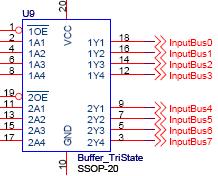
An example of the logical layout of schematic parts would be grouping
all the elements of buses together and in order, whereas the bus elements are
physically located further apart and out of order. The logical layout of an
8-bit buffer which feeds a bus labeled "inputBus" is shown for illustration.
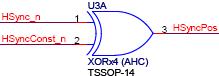
An example of using the logical function for a schematic part would
be to use a representation of function instead of the standard box with pins.
Part of the logical function of a chip containing four XOR gates is shown
for illustration. The part is numbered as U3A because the physical part U3
is logically represented by four XOR gates labeled U3A, U3B, U3C and U3D.
|
|
Layout Centric Schematics
Layout centric projects have their schematic parts formatted with a view
to the physical pinout.
An example of using the physical pinout for a schematic part would
be to use the standard box with pins format with the pins positioned and
numbered corresponding to their location on the physical chip.
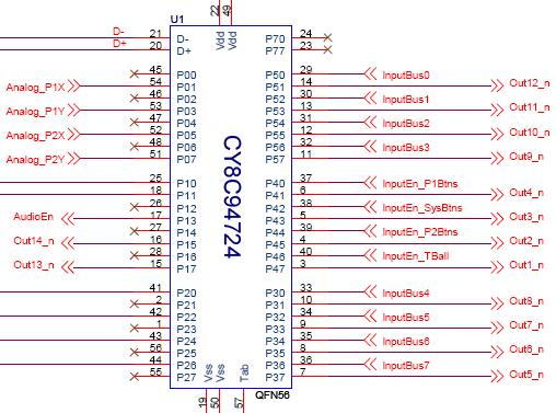
The illustration shown here of a Cypress USB microcontroller is a hybrid of
both the design and layout centric approaches. The schematic part was created
using the design centric approach. Each of the microcontroller's five 8-bit
buses are grouped together logically, despite their non-linear physical pin
positions. However, the signal design in the schematic is decidedly layout
centric: the 14 outputs are placed in 14 consecutive pins (3-16); the 8-bit
input bus is placed in 8 consecutive pins (29-36); the 4 input enables run on
the 4 pins following the input bus pins (37-40); finally, the analog bus is
also on 4 consecutive pins (51-54).
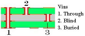 Spud Logic employs all available PCB design techniques as appropriate.
These techniques include: Via in pad, blind vias, buried vias, 5 mil trace
and spacing, custom PCB thickness (or thinness), and complex multi-layer
design. The different types of vias are illustrated to the right.
Spud Logic employs all available PCB design techniques as appropriate.
These techniques include: Via in pad, blind vias, buried vias, 5 mil trace
and spacing, custom PCB thickness (or thinness), and complex multi-layer
design. The different types of vias are illustrated to the right.
Advanced techniques are only used where absolutely necessary because they
add noise and/or design complexity. Spud Logic strives to produce PCBs with
the simplest implementation possible. This therefore keeps the production
costs down and the choice of fabrication houses wide open.
It is always desirable to produce the perfect layout. However, PCB layout
is a task with no end. It is always possible to nudge or re-route a trace
to make the plane areas bigger or reduce pinch points. It is always desirable
to examine all high-power or noisy lines for improved return paths. However,
all products have their design goals and restrictions. Through real world
experience, Spud Logic has realized the importance of making the effects of
the project parameters clear from the start of the design. PCB layout can
then be performed according to the project requirements, so the best use can
be made of the time available.
In addition to the complex programmable logic device (CPLD) technologies, of
which the FPGA is just one example, Spud Logic is happy to design using any
of the alternate programmable logic device (PLD) technologies (PLA, PAL, GAL,
etc.).
Perhaps one of the biggest surprises in the last ten years of semiconductor
development has been the evolution of FPGAs. This has been mainly due to the
soaring costs of designing and manufacturing ASICs. At one time, almost every
technology startup had an ASIC as part of its first product. However, those
lofty goals of ASIC design have mostly been replaced with more realistic and
cost-effective solutions using off-the-shelf microprocessors, microcontrollers
or DSPs. In the rare case where a custom ASIC is unavoidable, almost without
exception, the first product is implemented as a proof-of-concept in an FPGA.
Many successful products never make it into the intended ASIC and have a very
successful life using that very same prototype FPGA.
Spud Logic has experience implementing new and refurbishing old FPGA designs
in both VHDL and Verilog.
The cost of microcontrollers has plummeted in recent years. It is now possible
to buy single processors for just a couple of dollars, and that price is
reduced to just a few cents for larger quantities. Where many designs once
included discrete logic, counters, analog converters, etc. those very same
designs now have these functions built into the microcontroller.
Spud Logic is happy to include any microcontroller that is specified. However,
Spud Logic has a long term relationship with Cypress Semiconductor and their
family of PSoC microcontrollers. These controllers are available in a wide
range of sizes and configurations. They are re-programmable and run-time
configurable. Amongst other things, these devices may include one or more of:
ADC, DAC, Analog Comparator, Counter, Logic (AND, OR, XOR, NAND, etc.), and
much more. Hardware support is also provided for the following communication
protocols: USB, UART and I2C.
Spud Logic specializes in low level cycle accurate programming where known
execution times are required and enforced. An example of a cycle accurate
Spud Logic design is a system that detects the X/Y position on a monitor
running anything from CGA (240x320 73.6ns pixel rate) to XGA video (1024x768
15.3ns pixel rate). The interrupt routine to get candidate X/Y positions had
to run at less than the fastest line rate, which was 20.5us. With the amount
of processing required and the number of instructions available, the result
was a very intricately constructed piece of microcode requiring many
optimizations and branch balancing to save every possible cycle.
Many of today's ASICs contain a whole eco-system of what used to be discrete
processing elements. The embedded processor is becoming the normal occurrence
in many of these ASICs. The embedded processor will run a real-time operating
system (RTOS), which controls the execution of the many independent on-chip
functions.
In my humble opinion (disclaimer), the most common of these RTOS' is Linux,
with Wind River being the past master, and Microsoft trying to break into this
low mark-up, but exceedingly high volume market.
Spud Logic can help with many facets of the embedded processor world: the
configuration and integration of functions into an embedded environment; the
integration of the ASIC and any associated flash memory into a PCB system;
or the configuration of an existing embedded ASIC.
Home
About us
Services
Tour
Contact us